
Project brief
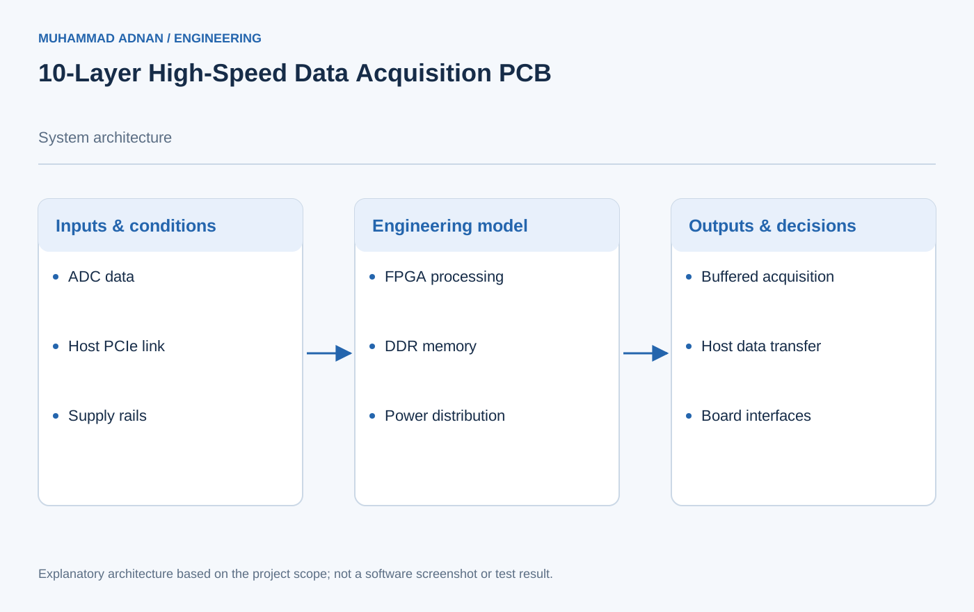
A complex 10-layer hybrid PCB (Rogers 4350B + FR4) for a high-speed data acquisition board. The design features DDR4-3200 memory interface using fly-by topology with optimized trace length matching, PCIe Gen 3 ×4 at 8Gbps per lane with AC coupling and controlled differential impedance, JESD204B ADC interface at 1GSPS, and a Xilinx UltraScale FPGA as the central processing element.
The scope emphasizes layout discipline, interface planning, and analysis for a high-speed acquisition board. No new eye diagrams or measured margins are asserted.
The engineering challenge
Route high-speed digital, RF, and power functions within a complex multilayer board stackup.
Engineering approach
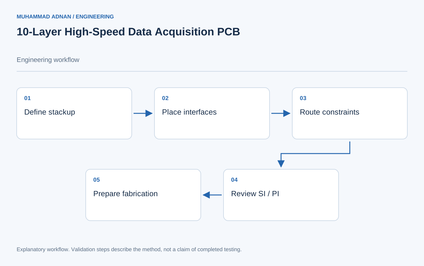
- Define interface routing constraints and return-path continuity.
- Coordinate memory, converter, and host-link placement around the FPGA.
- Use the stated signal- and power-integrity analyses to review layout choices.
Features & capabilities
- DDR4-3200 interface: fly-by topology, 20-mil trace matching, T-routing
- PCIe Gen 3 ×4 at 8Gbps: 100Ω differential, AC coupling, reference spreading
- JESD204B subclass 1: 12-bit, 1GSPS ADC (LTC2158-14) interface
- Controlled impedance: 50Ω SE ±10%, 100Ω differential ±10%
- 12 independent power domains with PDN analysis and decoupling optimization
- Ansys SIwave SI/PI analysis — pre and post-layout correlation
- 4-layer ground plane arrangement for minimal loop inductance
- Via-in-pad with back-drilling for signal integrity at >5GHz frequencies
Software & engineering tools
Altium Designer 23, Ansys SIwave, Rogers 4350B + FR4 stackup, 10-layer (1oz/oz/0.5oz), Xilinx UltraScale+, LTC2158