Project brief
A custom FPGA development platform based on the Xilinx Zynq-7020 SoC targeting aerospace signal processing research. The board features high-speed DDR3 memory, dual SFP+ ports for 10Gbps fiber networking, a 1GSPS 16-bit ADC input chain, programmable DC power supplies, and comprehensive debug interfaces including JTAG and UART.
The source presents a development-board specification. The expanded explanation should support a design discussion without implying independent verification of every component-interface pairing.
The engineering challenge
Provide a reusable FPGA research platform with acquisition, memory, expansion, and accessible debugging.
Engineering approach
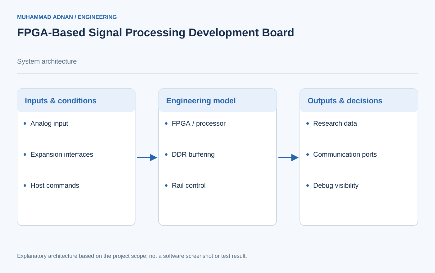
- Group converter input, FPGA processing, and memory into the core data path.
- Expose expansion and communications interfaces for experiments.
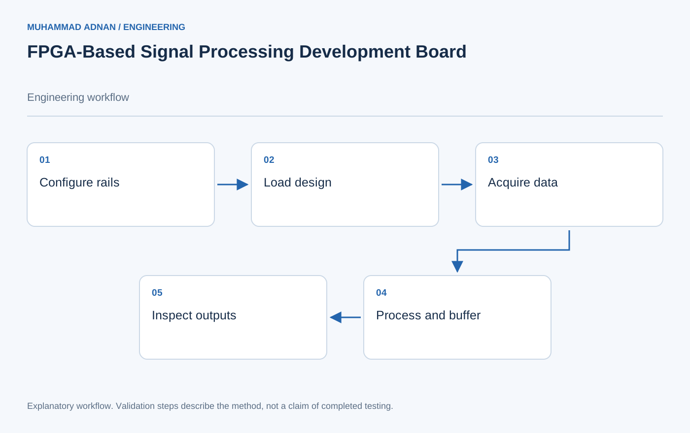
- Incorporate programmable rails and debug access for board bring-up.
Features & capabilities
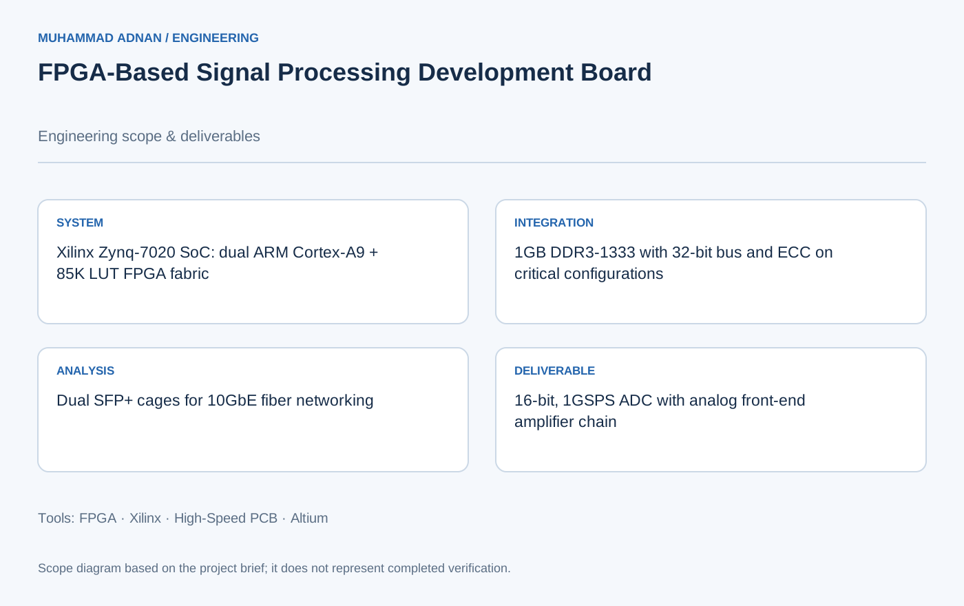
- Xilinx Zynq-7020 SoC: dual ARM Cortex-A9 + 85K LUT FPGA fabric
- 1GB DDR3-1333 with 32-bit bus and ECC on critical configurations
- Dual SFP+ cages for 10GbE fiber networking
- 16-bit, 1GSPS ADC with analog front-end amplifier chain
- Six programmable DC rails from 0.6V–5.5V (PMBus controlled)
- 6-layer stackup with 100Ω differential DDR and 50Ω RF traces
- FMC LPC connector for daughterboard daughter-card expansion
- Comprehensive debug: JTAG, UART, USB-UART bridge, GPIO LEDs
Software & engineering tools
Altium Designer, Xilinx Vivado/SDK, ADS5400 ADC, SI5351C clock gen, LTM4650 PMBus regulators, 6-layer PCB