Project brief
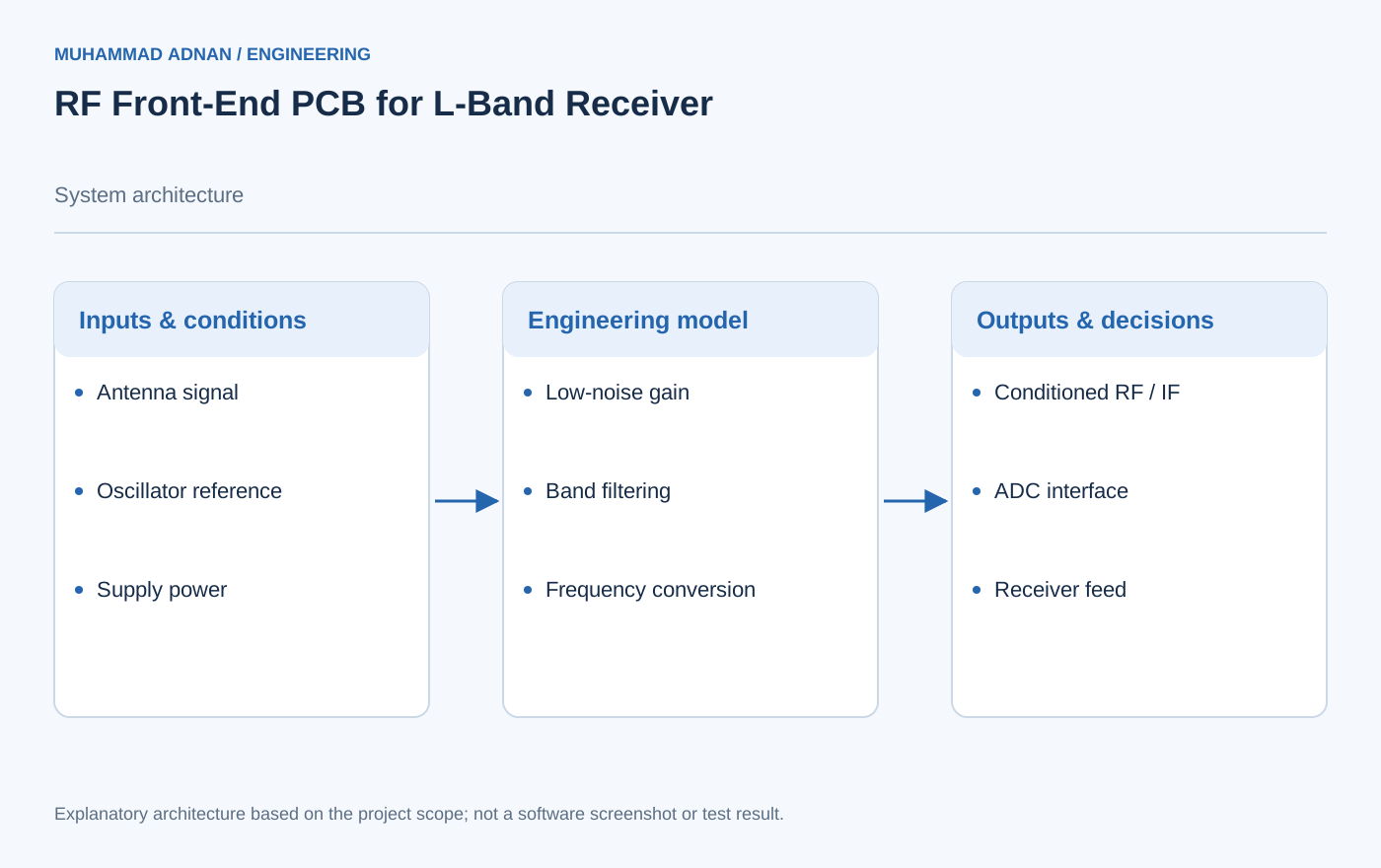
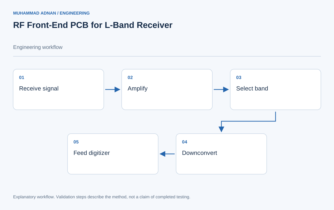
A high-performance RF front-end PCB for L-band satellite navigation receivers (GPS, GLONASS, Galileo, BeiDou L1/L2/L5). The board includes a cryogenic-capable LNA with 0.5dB noise figure, custom cavity bandpass filter, image reject mixer, and local oscillator chain, implementing the entire analog front end between antenna and ADC.
The record describes the analog path between antenna and digitizer, with RF layout and enclosure decisions forming part of the integration story.
The engineering challenge
Preserve weak navigation signals through amplification, filtering, frequency conversion, and board-level packaging.
Engineering approach
- Arrange RF gain, filtering, and mixing stages around the intended receive bands.
- Coordinate oscillator reference and analog output interfaces.
- Address impedance control and shielding in the physical board design.
Features & capabilities
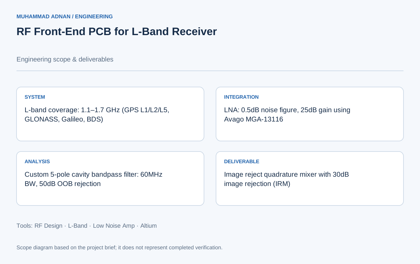
- L-band coverage: 1.1–1.7 GHz (GPS L1/L2/L5, GLONASS, Galileo, BDS)
- LNA: 0.5dB noise figure, 25dB gain using Avago MGA-13116
- Custom 5-pole cavity bandpass filter: 60MHz BW, 50dB OOB rejection
- Image reject quadrature mixer with 30dB image rejection (IRM)
- Integrated TCXO oscillator (±0.1ppm, ±25°C) for LO reference
- Rogers 4350B / Rogers 4003C laminate for RF signal layers
- Controlled impedance 50Ω ±5% all RF traces, SMA connectors
- Shielding: machined aluminum cover with EMI gasket seal
Software & engineering tools
Rogers 4350B, Altium Designer, Avago MGA-13116 LNA, HMC554 mixer, 4-layer RF PCB, Keysight VNA validation