

Project brief
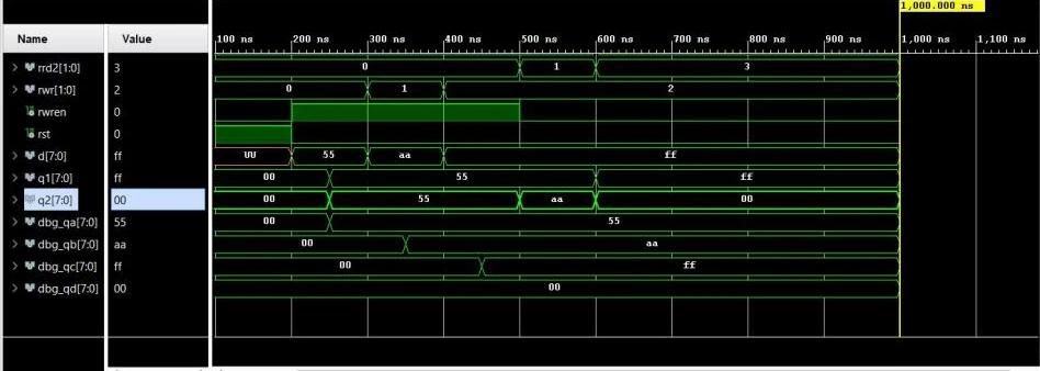
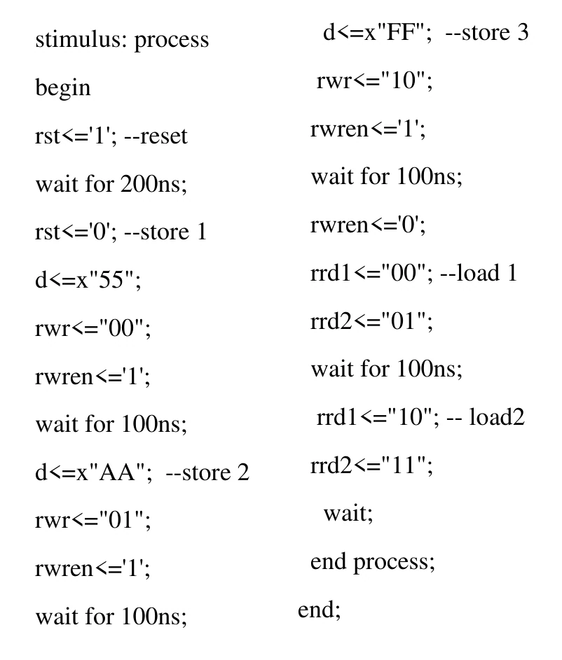
This project documents a VHDL verification exercise for a small processor register bank. The component interface exposes two read-address inputs, one write-address input, an eight-bit data input, two eight-bit read outputs and four register debug outputs. A separate testbench instantiates that component, generates a clock and applies a timed sequence of reset, write and read operations. The written stimulus loads hexadecimal 55, AA and FF into three selected registers, disables writes, and changes the two read addresses to inspect stored values. A Vivado Simulator waveform provides direct evidence of the resulting signal activity and register contents. The report connects this practical HDL work with an educational processor discussion covering instruction fetch, decode and execution, assembly operations, addressing modes and state encoding. Its strongest portfolio evidence is the relationship between interface definition, test stimulus and visible waveform behavior. The code uses explicit timing and named port mapping, which make the intended sequence easy to follow. This is a bounded simulation exercise: the document does not provide hardware deployment, timing closure, coverage statistics or an automated assertion suite. The project therefore demonstrates digital interface modeling and manual simulation inspection rather than a fully verified processor implementation.
The engineering challenge
Exercise the storage and dual-read behavior of a processor register bank with a clear, repeatable stimulus sequence and observable internal state.
Engineering approach
- Declare the register-bank component using IEEE standard logic types and eight-bit data buses.
- Instantiate the design under test with explicit named port mapping.
- Generate a clock using two 50 ns waits and apply the documented reset sequence.
- Write three hexadecimal test patterns, disable writes and select two register pairs for reading.
- Inspect the simulator waveform alongside the code and register debug outputs.
Results & observations
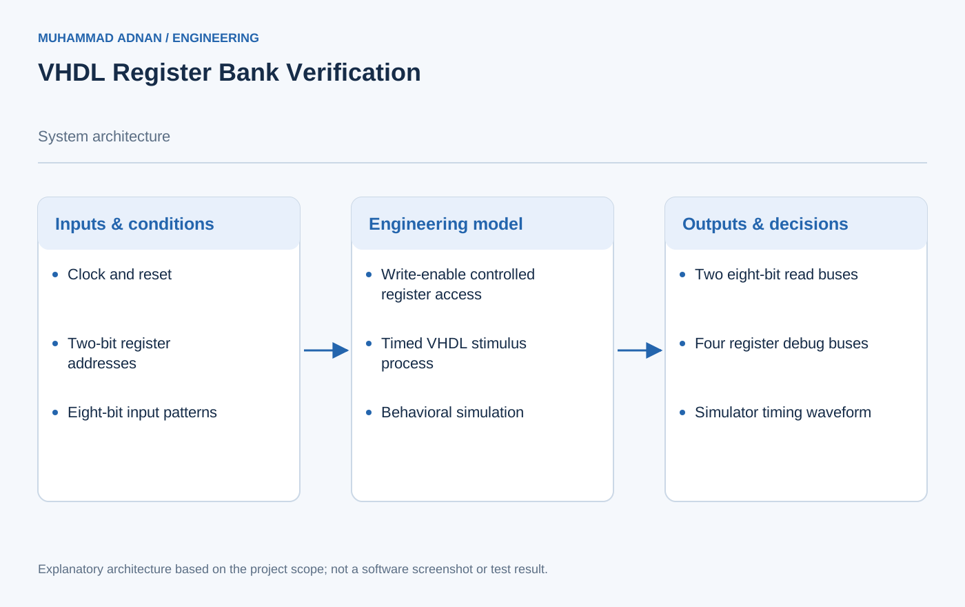
Four eight-bit debug outputs expose the register contents; two read ports share a single write interface.
The testbench assigns low and high clock levels for 50 ns each.
Hexadecimal data values applied to write addresses 00, 01 and 10 in the supplied stimulus.
The source screenshot displays stored values 55, AA, FF and 00 on the four register debug outputs.
Features & capabilities
- VHDL component interface
- Named port mapping
- Timed clock and reset
- Sequential register writes
- Dual read-port stimulus
- Register waveform inspection
Software & engineering tools
VHDL, Vivado Simulator 2019.1, IEEE Std_logic_1164, IEEE Numeric_Std